AT88SC1003 查看數據表(PDF) - Atmel Corporation
零件编号
产品描述 (功能)
生产厂家
AT88SC1003 Datasheet PDF : 30 Pages
| |||
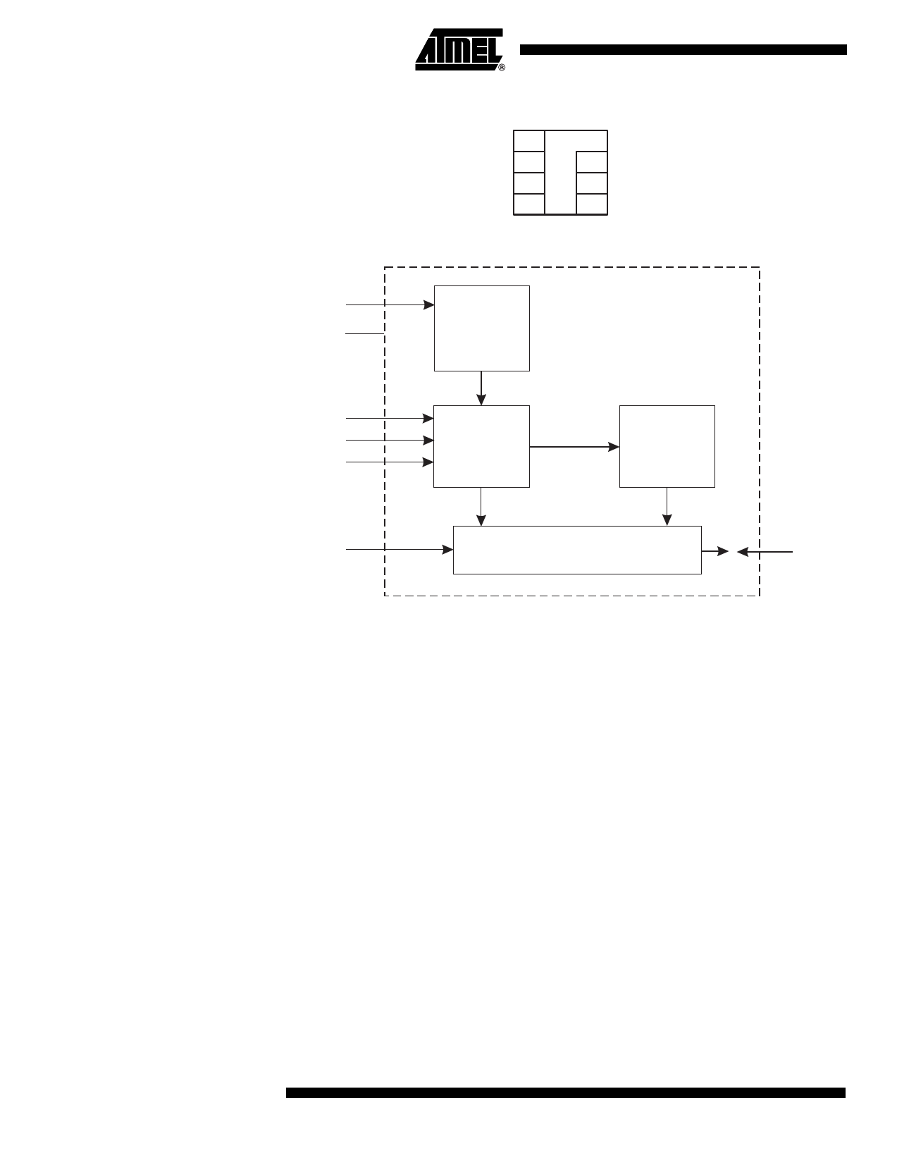
Figure 1. Card Module Contact
VCC = C1
RST = C2
CLK = C3
FUS = C4
Figure 2. Block Diagram
VCC
GND
Power On
Reset
RST
CLK
PGM
Address
Counter
C5 = GND
C6 = NC
C7 = I/O
C8 = PGM
E2PROM
Memory
FUS
Security Logic
I/O
Pin Descriptions
Supply Voltage (VCC)
Serial Clock (CLK)
Serial Data (I/O)
Reset (RST)
Program (PGM)
Fuse (FUS)
The VCC input is a 4.5V-to-5.5V positive voltage.
The CLK input is used to positive edge clock data into the device and negative edge
clock data out of the device. There is an internal pull-down on CLK.
I/O is bidirectional for serial data transfer to and from the device.
The RST input is used to reset the address counter. There is an internal pull-up on RST.
The PGM input is used to determine the state of I/O as an input or output. There is an
internal pull-down on PGM.
The FUS input is used during the personalization of the device. There is an internal pull-
down on FUS.
2 AT88SC1003
2035B–SMEM–08/03
Share Link: 