LTC1700_ 查看數據表(PDF) - Linear Technology
零件编号
产品描述 (功能)
生产厂家
LTC1700_ Datasheet PDF : 32 Pages
| |||
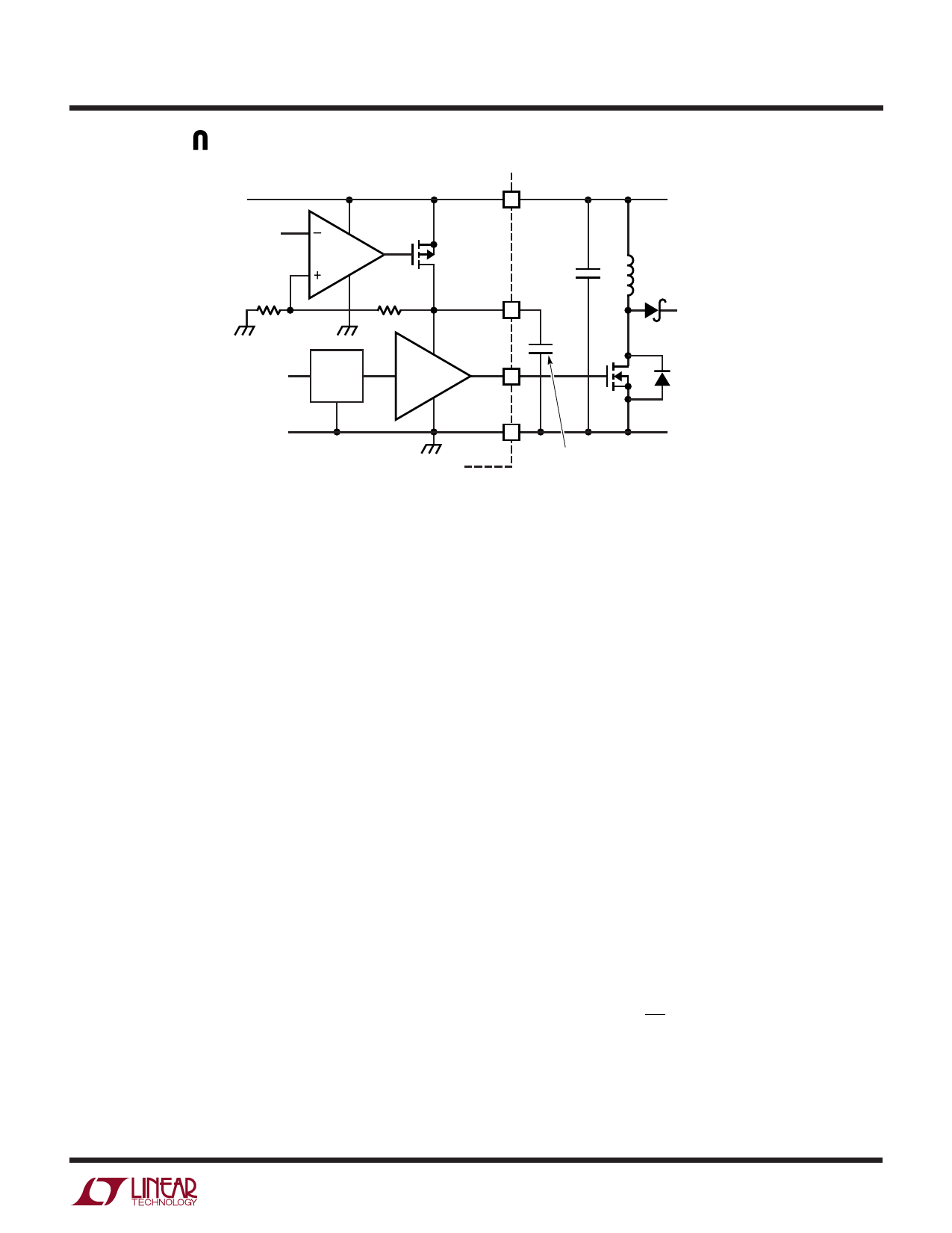
U
OPERATIO
LTC1871-7
–
1.230V
+
R2
VIN
P-CH
R1
7V INTVCC
INPUT
SUPPLY
2.5V TO 30V
CIN
LOGIC
DRIVER
GATE
CVCC
4.7µF
X5R
6V-RATED
M1
POWER
MOSFET
GND
18717 F07
GND
PLACE AS CLOSE AS
POSSIBLE TO DEVICE PINS
Figure 7. Bypassing the LDO Regulator and Gate Driver Supply
cause the LTC1871-7 to exceed its maximum junction
temperature rating. The junction temperature can be
estimated using the following equations:
IQ(TOT) ≈ IQ + f • QG
PIC = VIN • (IQ + f • QG)
TJ = TA + PIC • RTH(JA)
The total quiescent current IQ(TOT) consists of the static
supply current (IQ) and the current required to charge and
discharge the gate of the power MOSFET. The 10-pin
MSOP package has a thermal resistance of RTH(JA) =
120°C/W.
As an example, consider a power supply with VIN =10V.
The switching frequency is 200kHz, and the maximum
ambient temperature is 70°C. The power MOSFET chosen
is the FDS3670(Fairchild), which has a maximum RDS(ON)
of 35mΩ (at room temperature) and a maximum total gate
charge of 80nC (the temperature coefficient of the gate
charge is low).
IQ(TOT) = 600µA + 80nC • 200kHz = 16.6mA
PIC = 10V • 16.6mA = 166mW
TJ = 70°C + 120°C/W • 166mW = 89.9°C
TJRISE = 19.9°C
This demonstrates how significant the gate charge current
can be when compared to the static quiescent current in
the IC.
To prevent the maximum junction temperature from being
exceeded, the input supply current must be checked when
operating in a continuous mode at high VIN. A tradeoff
between the operating frequency and the size of the power
MOSFET may need to be made in order to maintain a
reliable IC junction temperature. Prior to lowering the
operating frequency, however, be sure to check with
power MOSFET manufacturers for their latest-and-great-
est low QG, low RDS(ON) devices. Power MOSFET manu-
facturing technologies are continually improving, with
newer and better performance devices being introduced
almost yearly.
Output Voltage Programming
The output voltage is set by a resistor divider according to
the following formula:
VO
=
1.230V
• 1+
R2
R1
The external resistor divider is connected to the output as
shown in Figure 1, allowing remote voltage sensing. The
18717f
11
Share Link: 