LTC690 查看數據表(PDF) - Linear Technology
零件编号
产品描述 (功能)
生产厂家
LTC690 Datasheet PDF : 18 Pages
| |||
LTC690/LTC691
LTC694/LTC695
APPLICATIONS INFORMATION
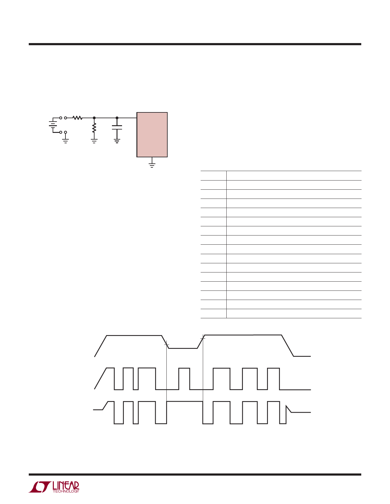
If battery connections are made through long wires, a
10Ω to 100Ω series resistor and a 0.1μF capacitor are
recommended to prevent any overshoot beyond VCC due
to the lead inductance (Figure 4).
10Ω
4.3M
0.1μF
VBATT
LTC690
LTC691
LTC694
LTC695
GND
690 F04
Figure 4. 10Ω/0.1μF Combination Eliminates Inductive
Overshoot and Prevents Spurious Resets During Battery
Replacement
Table 1 shows the state of each pin during battery back-up.
When the battery switchover section is not used, connect
VBATT to GND and VOUT to VCC.
Memory Protection
The LTC691 and LTC695 include memory protection
circuitry that ensures the integrity of the data in memory
by preventing write operations when VCC is at invalid level.
Two additional pins, CE IN and CE OUT, control the Chip
Enable or Write inputs of CMOS RAM. When VCC is 5V,
CE OUT follows CE IN with a typical propagation delay of
20ns. When VCC falls below the reset voltage threshold
or VBATT, CE OUT is forced high, independent of CE IN. CE
OUT is an alternative signal to drive the CE, CS, or Write
input of battery-backed up CMOS RAM. CE OUT can also
be used to drive the Store or Write input of an EEPROM,
EAROM or NOVRAM to achieve similar protection. Figure
5 shows the timing diagram of CE IN and CE OUT.
CE IN can be derived from the microprocessor’s address
decoder output. Figure 6 shows a typical nonvolatile CMOS
RAM application.
Memory protection can also be achieved with the LTC690
and LTC694 by using RESET as shown in Figure 7.
Table 1. Input and Output Status in Battery Back-Up Mode
SIGNAL STATUS
VCC
VOUT
VBATT
BATT ON
PFI
PFO
RESET
C2 monitors VCC for active switchover.
VOUT is connected to VBATT through an internal PMOS switch.
The supply current is 1μA maximum.
Logic high. The open-circuit output voltage is equal to VOUT.
Power failure input is ignored.
Logic low
Logic low
RESET Logic high. The open-circuit output voltage is equal to VOUT.
LOW⎯LINE Logic low
WDI
WDO
CE IN
CE OUT
OSC IN
Watchdog input is ignored.
Logic high. The open-circuit output voltage is equal to VOUT.
Chip⎯Enable Input is ignored.
Logic high. The open-circuit output voltage is equal to VOUT.
OSC IN is ignored.
OSC SEL OSC SEL is ignored.
V2
VCC
V1
V1 = RESET VOLTAGE THRESHOLD
V2 = RESET VOLTAGE THRESHOLD +
RESET THRESHOLD HYSTERESIS
CE IN
CE OUT
VOUT = VBATT
Figure 5. Timing Diagram for CE IN and CE OUT
VOUT = VBATT
690 F05
690fe
11
Share Link: 