W77E516 查看數據表(PDF) - Winbond
零件编号
产品描述 (功能)
生产厂家
W77E516 Datasheet PDF : 85 Pages
| |||
Preliminary W77E516
ISP Data Buffer
Bit:
7
6
5
4
3
2
1
0
D7
D6
D5
D4
D3
D2
D1
D0
Mnemonic: SFRFD
Address: AEh
In ISP mode, read/write a specific byte ROM content must go through SFRFD register.
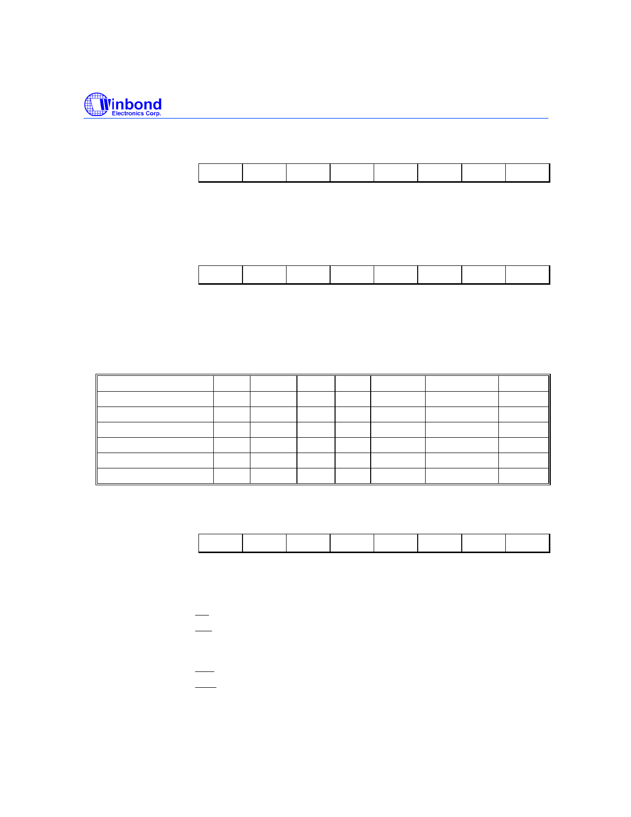
ISP Operation Modes
Bit:
7
6
5
WFWIN NOE
4
3
2
1
0
NCE CTRL3 CTRL2 CTRL1 CTRL0
Mnemonic: SFRCN
Address: AFh
WFWIN: Destination ROM bank for programming, erasure and read. 0 = APROM, 1 = LDROM.
NOE: Flash EPROM output enable.
NCE: Flash EPROM chip enable.
CTRL[3:0]: Mode Selection.
ISP Mode
Erase 4KB LDROM
Erase 64K APROM
Program 4KB LDROM
Program 64KB APROM
Read 4KB LDROM
Read 64KB APROM
BANK
0
0
0
0
0
0
WFWIN
1
0
1
0
1
0
NOE
1
1
1
1
0
0
NCE
0
0
0
0
0
0
CTRL<3:0>
0010
0010
0001
0001
0000
0000
SFRAH, SFRAL
X
X
Address in
Address in
Address in
Address in
SFRFD
X
X
Data in
Data in
Data out
Data out
Port 3
Bit:
7
6
5
4
3
2
1
0
P3.7 P3.6 P3.5 P3.4 P3.3 P3.2 P3.1 P3.0
Mnemonic: P3
Address: B0h
P3.7 - 0: General purpose I/O port. Each pin also has an alternate input or output function. The
alternate functions are described below.
P3.7
P3.6
P3.5
P3.4
P3.3
P3.2
P3.1
P3.0
RD
WR
T1
T0
INT1
INT0
TxD
RxD
Strobe for read from external RAM
Strobe for write to external RAM
Timer/counter 1 external count input
Timer/counter 0 external count input
External interrupt 1
External interrupt 0
Serial port 0 output
Serial port 0 input
- 23 -
Publication Release Date: August 16, 2002
Revision A1
Share Link: 