PSD834F2-10J 查看數據表(PDF) - STMicroelectronics
零件编号
产品描述 (功能)
生产厂家
PSD834F2-10J
STMicroelectronics

PSD834F2-10J Datasheet PDF : 95 Pages
| |||
PSD834F2V
Data Toggle. Checking the Toggle Flag (DQ6) The Error Flag (DQ5) Bit is set if either an internal
Bit is a method of determining whether a Program time-out occurred while the embedded algorithm
or Erase cycle is in progress or has completed. attempted to program the byte, or if the MCU at-
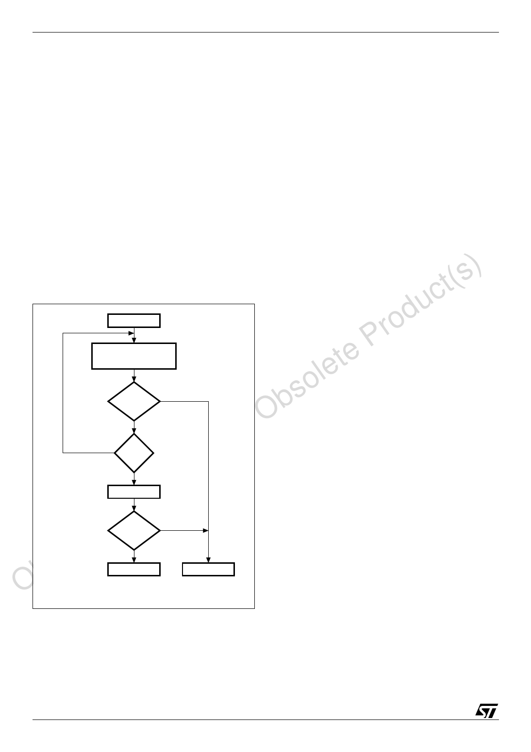
Figure 5 shows the Data Toggle algorithm.
tempted to program a '1' to a bit that was not
When the MCU issues a Program instruction, the erased (not erased is logic '0').
embedded algorithm within the PSD begins. The It is suggested (as with all Flash memories) to read
MCU then reads the location of the byte to be pro- the location again after the embedded program-
grammed in Flash memory to check status. The ming algorithm has completed, to compare the
Toggle Flag (DQ6) Bit of this location toggles each byte that was written to Flash memory with the
time the MCU reads this location until the embed- byte that was intended to be written.
ded algorithm is complete. The MCU continues to When using the Data Toggle method after an
read this location, checking the Toggle Flag (DQ6) Erase cycle, Figure 5 still applies. the Toggle Flag
Bit and monitoring the Error Flag (DQ5) Bit. When (DQ6) Bit toggles until the Erase cycle is complete.
the Toggle Flag (DQ6) Bit stops toggling (two con- A 1 on the Error Flag (DQ5) Bit indicates a time-out
secutive READs yield the same value), and the Er- condition on the Erase cycle; a 0 indicates no er-
ror Flag (DQ5) Bit remains '0,' the embedded ror. The MCU can read any location within the sec-
algorithm is complete. If the Error Flag (DQ5) Bit is tor being erased to get the Toggle Flag (DQ6) Bit
'1,' the MCU should test the Toggle Flag (DQ6) Bit and the Error Flag (DQ5) Bit.
again, since the Toggle Flag (DQ6) Bit may have
changed simultaneously with the Error Flag (DQ5)
) Bit (see Figure 5).
ct(s Figure 5. Data Toggle Flowchart
du START
Pro READ
te DQ5 & DQ6
sole DQ= 6
NO
TOGGLE
Ob YES
t(s) - NO DQ5
=1
c YES
du READ DQ6
Pro DQ= 6
NO
teTOGGLE
le YES
Obso FAIL
PASS
PSDsoft Express generates ANSI C code func-
tions which implement these Data Toggling algo-
rithms.
Unlock Bypass. The Unlock Bypass instructions
allow the system to program bytes to the Flash
memories faster than using the standard Program
instruction. The Unlock Bypass mode is entered
by first initiating two Unlock cycles. This is followed
by a third WRITE cycle containing the Unlock By-
pass code, 20h (as shown in Table 7).
The Flash memory then enters the Unlock Bypass
mode. A two-cycle Unlock Bypass Program in-
struction is all that is required to program in this
mode. The first cycle in this instruction contains
the Unlock Bypass Program code, A0h. The sec-
ond cycle contains the program address and data.
Additional data is programmed in the same man-
ner. These instructions dispense with the initial
two Unlock cycles required in the standard Pro-
gram instruction, resulting in faster total Flash
memory programming.
During the Unlock Bypass mode, only the Unlock
Bypass Program and Unlock Bypass Reset Flash
instructions are valid.
To exit the Unlock Bypass mode, the system must
issue the two-cycle Unlock Bypass Reset Flash in-
struction. The first cycle must contain the data
90h; the second cycle the data 00h. Addresses are
Don’t Care for both cycles. The Flash memory
then returns to READ Mode.
AI01370B
20/95
Share Link: