C5002 查看數據表(PDF) - Cypress Semiconductor
零件编号
产品描述 (功能)
生产厂家
C5002 Datasheet PDF : 16 Pages
| |||
C5002
Low Skew Multiple Frequency PCI Clock Generator with EMI Reducing SSCG
Approved Product
Product Features
§ Produces PCI output clocks that are individually
selectable for 33.3 or 66.6 MHz under SMBus or
strapping control.
§ Separate output buffer power supply for reduced
noise, crosstalk and jitter.
§ input clock frequency standard 14.31818 MHz
§ Output clocks frequency individually selectable via
SMBus or hardware bi-directional pin strapping.
§ SSCG EMI reduction at 1.0% width
§ Individual clock disables via SMBus control
§ All output clocks skewed within a 500 pS window
§ Cycle to Cycle jitter ± 250 pS
§ Output duty cycle is automatically 50% (±10%)
adjusted
§ Clock feed through mode and OE pins for logic
testing
§ Glitchless clock enabling and disabling transitions
§ 28-pin TSSOP or SSOP package
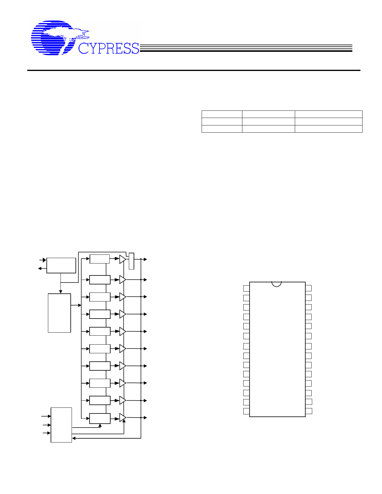
Block Diagram
XIN
XOUT
Reference
Oscillator
÷1 ÷2
÷1 ÷2
M
U
REF-
X
CLK0/S0
CLK1/S
PLL
÷1 ÷2
÷1 ÷2
CLK2/S
2
CLK3/S3
÷1 ÷2
CLK4/S4
÷1 ÷2
CLK5/S5
÷1 ÷2
CLK6/S6
÷1 ÷2
CLK7/S7
÷1 ÷2
CLK8/S8
OE
SDATA
SCLK
SMBus
LOGIC
÷1 ÷2
÷4, ÷8
CLK9/S9
Cypress Semiconductor Corporation
525 Los Coches St.
Milpitas, CA 95035. Tel: 408-263-6300, Fax: 408-263-6571
http://www.cypress.com
Output Enable Logic Functionality Table
OE
CLK(0:9)
PLL
1 (HIGH)
Enabled
Running
0 (LOW)
Tri State
Stopped*
*See Output Enable Control section of this datasheet.
Pin Configuration
VDD 1
XIN 2
XOUT 3
VSS 4
OE 5
SCLK 6
SDATA 7
VSS 8
VSS 9
CLK9/S9 10
CLK8/S8 11
VDD5 12
VSS 13
CLK7/S7 14
28 VDD1
27 REF-CLK0/S0
26 CLK1/S1
25 VSS
24 VDD2
23 CLK2/S2
22 CLK3/S3
21 VSS
20 VDD3
19 CLK4/S4
18 CLK5/S5
17 VSS
16. VDD4
15 CLK6/S6
Document#: 38-07014 Rev. **
5/4/2001
Page 1 of 16
Share Link: 