C5002 查看數據表(PDF) - Cypress Semiconductor
零件编号
产品描述 (功能)
生产厂家
C5002 Datasheet PDF : 16 Pages
| |||
C5002
Low Skew Multiple Frequency PCI Clock Generator with EMI Reducing SSCG
Approved Product
Input and Output Relationships
The device acts a PCI clock generator. Output clocks may be individually controlled to be either 33.3 or 66.6 MHz in
frequency by setting or clearing the clocks respective SMBus control register bit. All output clocks are rising edge aligned
to within a shared 500 pS window. There is no specified relationship between the input reference clock and the output
clocks.
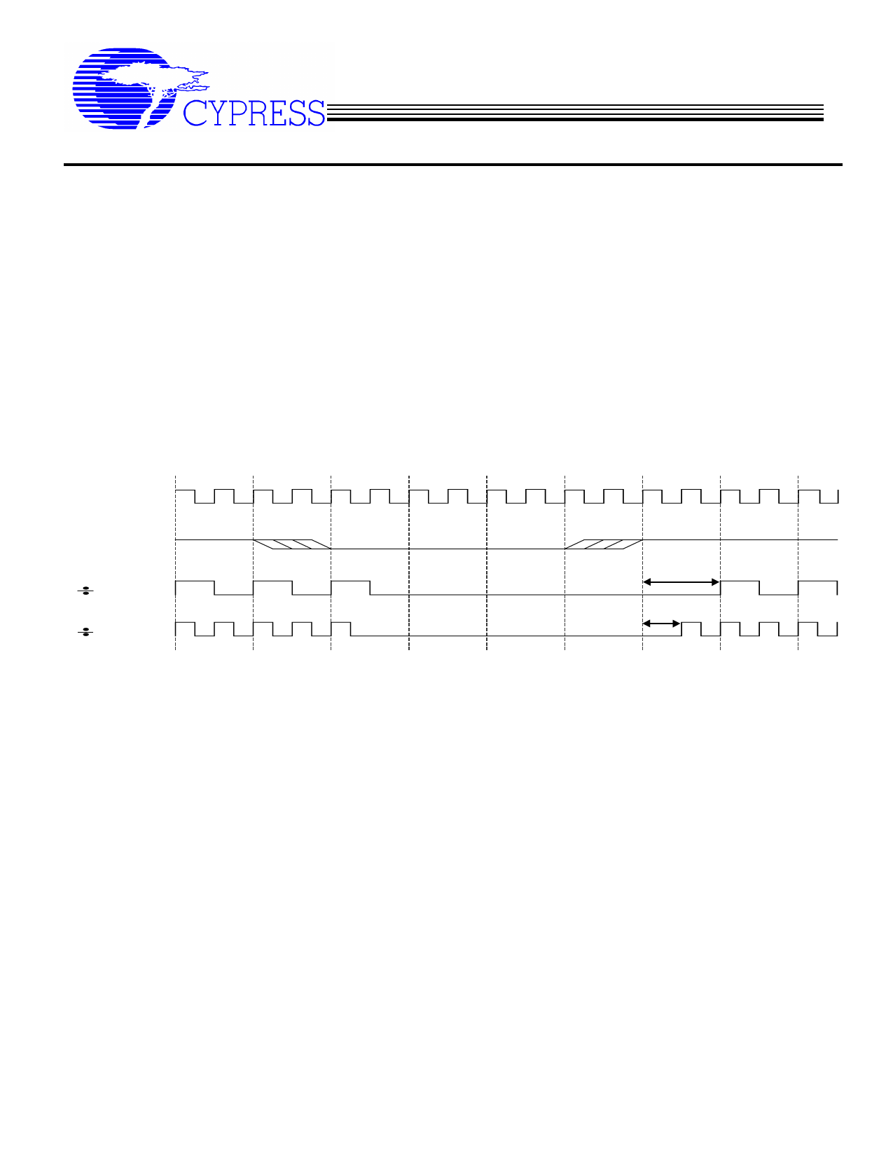
Clock Enable Functions and Timing
Each output clock may be either disabled or enabled by either setting or clearing its respective SMBus register control
bit.
All clocks are stopped in the low state. All clocks maintain a valid high period before transitioning from running to
stopped. The clocks transition between running and stopped occurs immediately after the SMBus register bit is cleared
and the clock transitions to a low state. See figure below.
Internal
Clock
I2C
Register
BIT
2 Output
1 Output
A
B
A: represents one output ÷2 clock cycle (one 33.3 MHZ cycle period).
B: represents one output clock ÷ 1 cycle (one 66.6 MHZ cycle period).
Output Frequency Change Relationships
The SMBus registers are initially set (initialized) by the voltage levels present on the clocks output pins at power up.
Subsequently these bits may be changed via SMBus commands.
Output clocks have the capability to be changed, on the fly, via the devices SMBus register bits. If Synchronous
switching is required, it may be achieved by first disabling a specific clock, changing its frequency and then re-enabling it
via the SMBus register control bits that are provided for these functions.
Synchronous switching is defines at the changing of the output frequency of a clock from one frequency to another in
such a manner as to not produce any clock cycles shorter than the higher of the 2 frequencies or longer than the period
of the lower of the 2 frequencies. The disable and enable SMBus register bit control of each clock is logically
implemented to eliminate clock glitches when each clock is either enabled or enabled.
Cypress Semiconductor Corporation
525 Los Coches St.
Milpitas, CA 95035. Tel: 408-263-6300, Fax: 408-263-6571
http://www.cypress.com
Document#: 38-07014 Rev. **
5/4/2001
Page 6 of 16
Share Link: 