MTP10N10E 查看數據表(PDF) - ON Semiconductor
零件编号
产品描述 (功能)
生产厂家
MTP10N10E Datasheet PDF : 8 Pages
| |||
30
10
VGS = 20 V
SINGLE PULSE
3 TC = 25°C
MTP10N10E
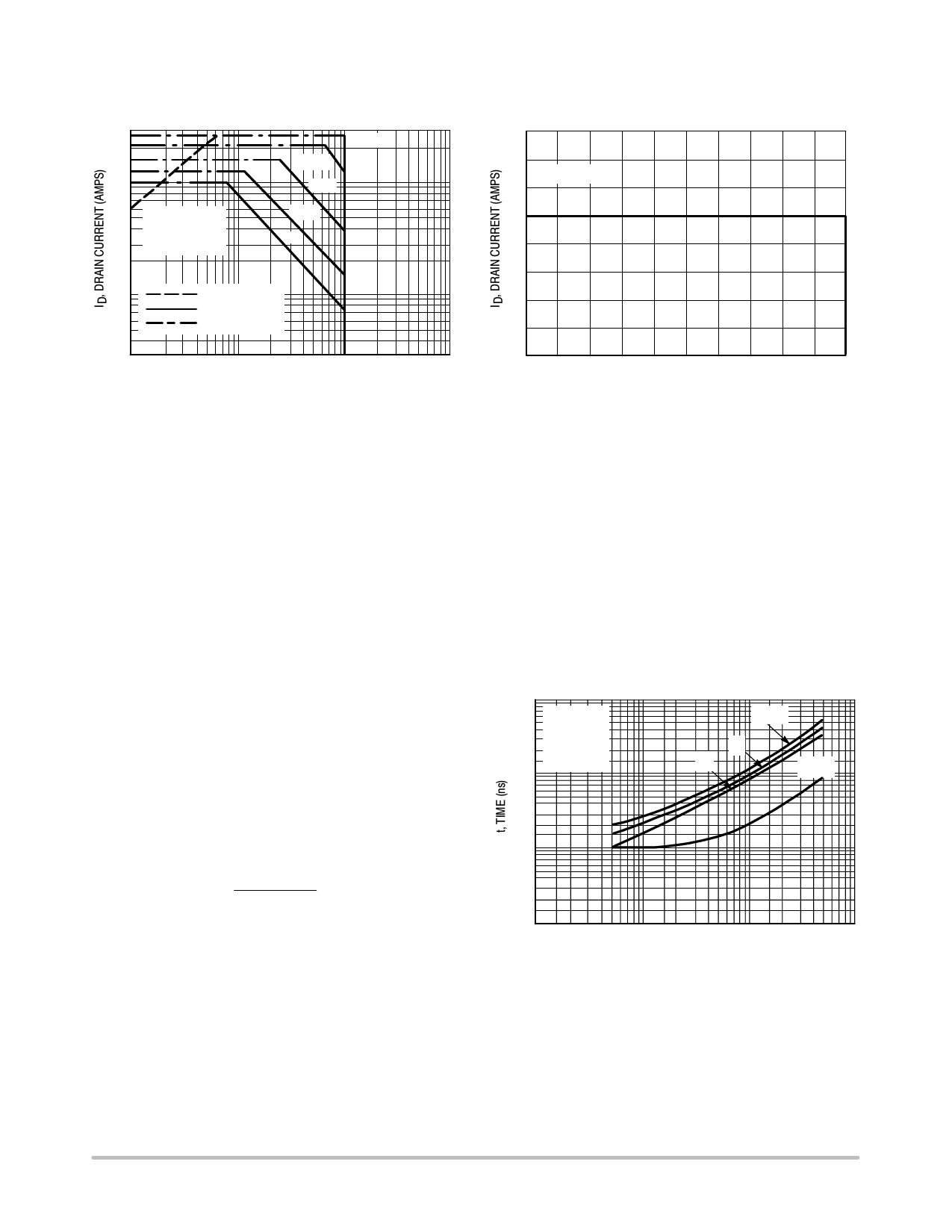
SAFE OPERATING AREA INFORMATION
10 µs
100 µs
1 ms
10 ms
dc
40
TJ ≤ 150°C
30
20
1
RDS(on) LIMIT
THERMAL LIMIT
PACKAGE LIMIT
0.3
1
10
100
VDS, DRAIN-TO-SOURCE VOLTAGE (VOLTS)
Figure 7. Maximum Rated Forward Biased
Safe Operating Area
10
0
0
20
40
60
80
100
VDS, DRAIN-TO-SOURCE VOLTAGE (VOLTS)
Figure 8. Maximum Rated Switching
Safe Operating Area
FORWARD BIASED SAFE OPERATING AREA
The FBSOA curves define the maximum drain–to–source
voltage and drain current that a device can safely handle
when it is forward biased, or when it is on, or being turned
on. Because these curves include the limitations of
simultaneous high voltage and high current, up to the rating
of the device, they are especially useful to designers of linear
systems. The curves are based on a case temperature of 25°C
and a maximum junction temperature of 150°C. Limitations
for repetitive pulses at various case temperatures can be
determined by using the thermal response curves. ON
Semiconductor Application Note, AN569, “Transient
Thermal Resistance–General Data and Its Use” provides
detailed instructions.
SWITCHING SAFE OPERATING AREA
The switching safe operating area (SOA) of Figure 8 is the
boundary that the load line may traverse without incurring
damage to the MOSFET. The fundamental limits are the
peak current, IDM and the breakdown voltage, V(BR)DSS.
The switching SOA shown in Figure 8 is applicable for both
turn–on and turn–off of the devices for switching times less
than one microsecond.
The power averaged over a complete switching cycle
must be less than:
TJ(max) – TC
RθJC
1K
500 VDD = 25 V
300
200
ID = 5 A
VGS = 10 V
100 TJ = 25°C
70
50
30
20
td(off)
tf
tr
td(on)
10
7
5
3
2
1
1 2 3 5 10 20 30 50 100 200 300 500 1K
RG, GATE RESISTANCE (OHMS)
Figure 9. Resistive Switching Time
versus Gate Resistance
http://onsemi.com
4
Share Link: 