ICS8531-01 查看數據表(PDF) - Integrated Device Technology
零件编号
产品描述 (功能)
生产厂家
ICS8531-01 Datasheet PDF : 18 Pages
| |||
ICS8531-01
LOW SKEW, 1-TO-9, DIFFERENTIAL-TO-3.3V LVPECL FANOUT BUFFER
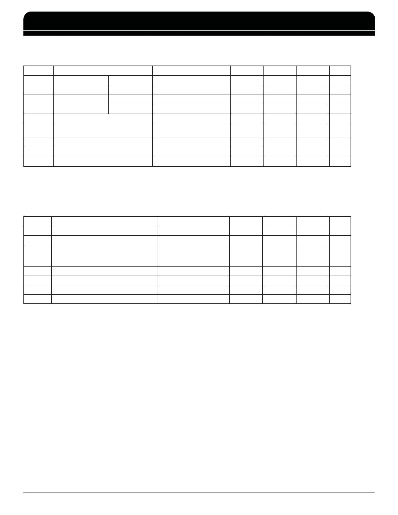
TABLE 4D. LVPECL DC CHARACTERISTICS, VCC = VCCO = 3.3V±5%, TA = 0°C TO 70°C
Symbol Parameter
Test Conditions
Minimum Typical
IIH
IIL
VPP
VCMR
PCLK
Input High Current
nPCLK
PCLK
Input Low Current
nPCLK
Peak-to-Peak Input Voltage
Common Mode Input Voltage;
NOTE 1, 2
VCC = VIN = 3.465V
V = V = 3.465V
CC
IN
VIN = 0V, VCC = 3.465V
VIN = 0V, VCC = 3.465V
-5
-150
0.3
VEE + 1.5
VOH
Output High Voltage; NOTE 3
VCCO - 1.4
VOL
Output Low Voltage; NOTE 3
VCCO - 2.0
VSWING
Peak-to-Peak Output Voltage Swing
0.6
NOTE 1: Common mode input voltage is defined as VIH.
NOTE 2: For single ended applications, the maximum input voltage for PCLK and nPCLK is VCC + 0.3V.
NOTE 3: Outputs terminated with 50Ω to VCCO - 2V.
Maximum
150
5
1
VCC
VCCO - 0.9
VCCO - 1.7
1.0
Units
µA
µA
µA
µA
V
V
V
V
V
TABLE 5. AC CHARACTERISTICS, VCC = VCCO = 3.3V±5%, TA = 0°C TO 70°C
Symbol Parameter
Test Conditions
Minimum Typical Maximum
fMAX
Output Frequency
tPD
Propagation Delay; NOTE 1
Buffer Additive Phase Jitter, RMS;
tjit
refer to Additive Phase Jitter Section;
NOTE 2
IJ 250MHz
155.52MHz,
(12kHz to 20MHz)
500
1
2
0.17
tsk(o) Output Skew; NOTE 3, 5
50
tsk(pp) Part-to-Part Skew; NOTE 4, 5
250
tR / tF
odc
Output Rise/Fall Time
Output Duty Cycle
20% to 80% @ 50MHz
300
700
48
50
52
All parameters measured at 250MHz unless noted otherwise.
NOTE 1: Measured from the differential input crossing point to the differential output crossing point.
NOTE 2: Driving only one input clock.
NOTE 3: Defined as skew between outputs at the same supply voltage and with equal load conditions.
Measured at the output differential cross points.
NOTE 4: Defined as skew between outputs on different devices operating at the same supply voltages
and with equal load conditions. Using the same type of inputs on each device, the outputs are measured
at the differential cross points.
NOTE 5: This parameter is defined in accordance with JEDEC Standard 65.
Units
MHz
ns
ps
ps
ps
ps
%
IDT™ / ICS™ 1-TO-9, 3.3V LVPECL FANOUT BUFFER
5
ICS8531AY-01 REV. F APRIL 11, 2007
Share Link: 