LTC1196 查看數據表(PDF) - Linear Technology
零件编号
产品描述 (功能)
生产厂家
LTC1196 Datasheet PDF : 28 Pages
| |||
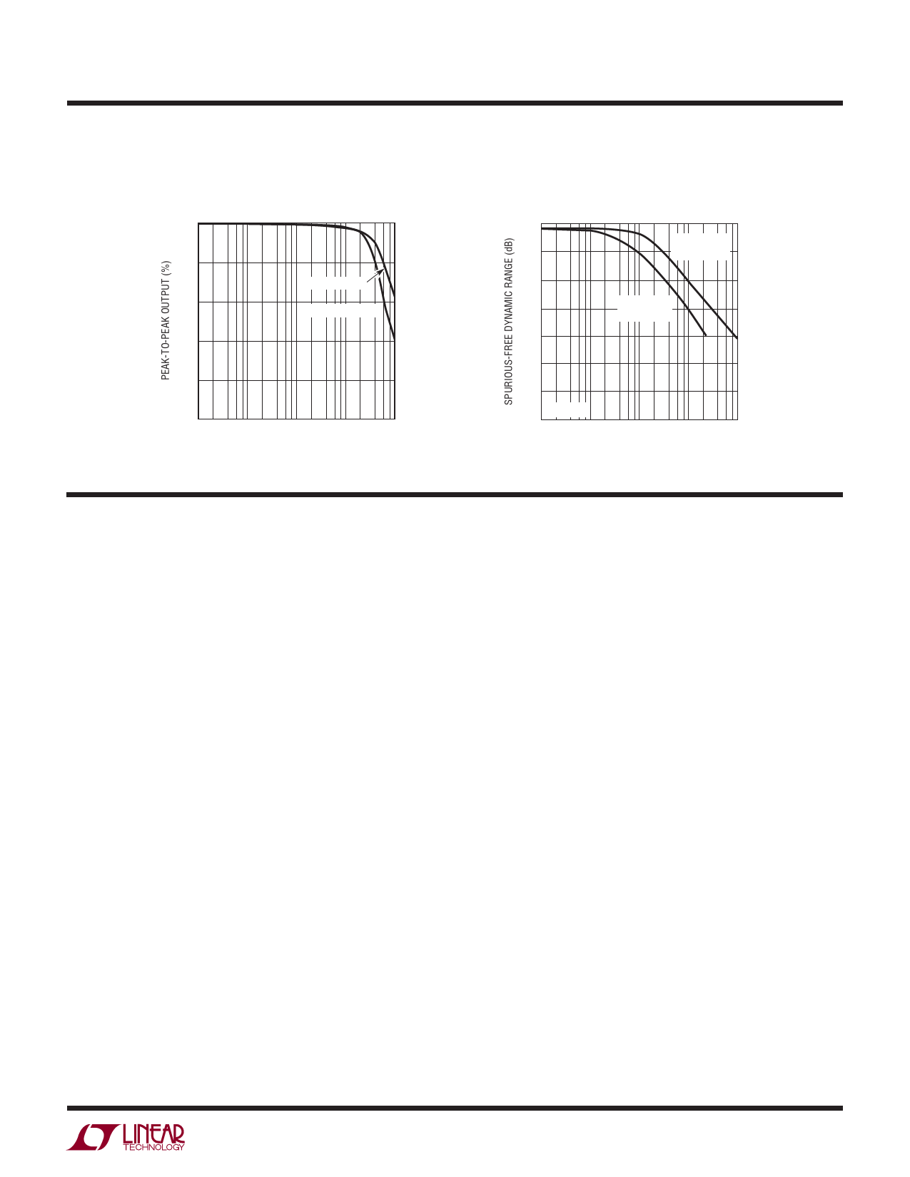
TYPICAL PERFORMANCE CHARACTERISTICS
LTC1196/LTC1198
Output Amplitude vs
Input Frequency
100
80
VREF = VCC = 5V
60
VREF = VCC = 2.7V
40
20
0
1k
10k
100k
1M
10M
INPUT FREQUENCY (Hz)
1196/98 G34
Spurious-Free Dynamic Range
vs Frequency
70
VCC = 5V
60
fCLK = 12MHz
50
40
VCC = 3V
fCLK = 5MHz
30
20
10
TA = 25°C
0
1k
10k
100k
1M
10M
FREQUENCY (Hz)
1196/98 G35
PIN FUNCTIONS
LTC1196
CS (Pin 1): Chip Select Input. A logic low on this input
enables the LTC1196. A logic high on this input disables
the LTC1196.
IN+ (Pin 2): Analog Input. This input must be free of noise
with respect to GND.
IN– (Pin 3): Analog Input. This input must be free of noise
with respect to GND.
GND (Pin 4): Analog Ground. GND should be tied directly
to an analog ground plane.
VREF (Pin 5): Reference Input. The reference input defines
the span of the A/D converter and must be kept free of
noise with respect to GND.
DOUT (Pin 6): Digital Data Output. The A/D conversion
result is shifted out of this output.
CLK (Pin 7): Shift Clock. This clock synchronizes the se-
rial data transfer.
VCC (Pin 8): Power Supply Voltage. This pin provides power
to the A/D converter. It must be kept free of noise and ripple
by bypassing directly to the analog ground plane.
LTC1198
CS/SHUTDOWN (Pin 1): Chip Select Input. A logic low
on this input enables the LTC1198. A logic high on this
input disables the LTC1198 and disconnects the power
to THE LTC1198.
CHO (Pin 2): Analog Input. This input must be free of
noise with respect to GND.
CH1 (Pin 3): Analog Input. This input must be free of noise
with respect to GND.
GND (Pin 4): Analog Ground. GND should be tied directly
to an analog ground plane.
DIN (Pin 5): Digital Data Input. The multiplexer address is
shifted into this input.
DOUT (Pin 6): Digital Data Output. The A/D conversion
result is shifted out of this output.
CLK (Pin 7): Shift Clock. This clock synchronizes the se-
rial data transfer.
VCC (VREF)(Pin 8): Power Supply and Reference Voltage.
This pin provides power and defines the span of the A/D
converter. It must be kept free of noise and ripple by by-
passing directly to the analog ground plane.
119698fa
11
Share Link: 