74LVC109D,118 查看數據表(PDF) - NXP Semiconductors.
零件编号
产品描述 (功能)
生产厂家
74LVC109D,118 Datasheet PDF : 18 Pages
| |||
Philips Semiconductors
Dual JK flip-flop with set and reset;
positive-edge trigger
Product specification
74LVC109
FEATURES
• 5 V tolerant inputs for interfacing with 5 V logic
• Wide supply voltage range from 1.2 to 3.6 V
• CMOS low power consumption
• Direct interface with TTL levels
• Inputs accept voltages up to 5.5 V
• Complies with JEDEC standard no. 8-1A
• ESD protection:
HBM EIA/JESD22-A114-A exceeds 2000 V
MM EIA/JESD22-A115-A exceeds 200 V.
• Specified from −40 to +85 °C and −40 to +125 °C.
DESCRIPTION
The 74LVC109A is a high-performance, low-voltage,
Si-gate CMOS device, superior to most advanced CMOS
compatible TTL families.
The 74LVC109A is a dual positive edge triggered
JK flip-flop featuring individual J and K inputs, clock (CP)
inputs, set (SD) and reset (RD) inputs and complementary
Q and Q outputs.
The set and reset are asynchronous active LOW inputs
and operate independently of the clock input.
The J and K inputs control the state changes of the
flip-flops as described in the mode select function table.
The J and K inputs must be stable one set-up time prior to
the LOW-to-HIGH clock transition for predictable
operation. The JK design allows operation as a D-type
flip-flop by tying the J and K inputs together.
Schmitt-trigger action in the clock input makes the circuit
highly tolerant to slower clock rise and fall times.
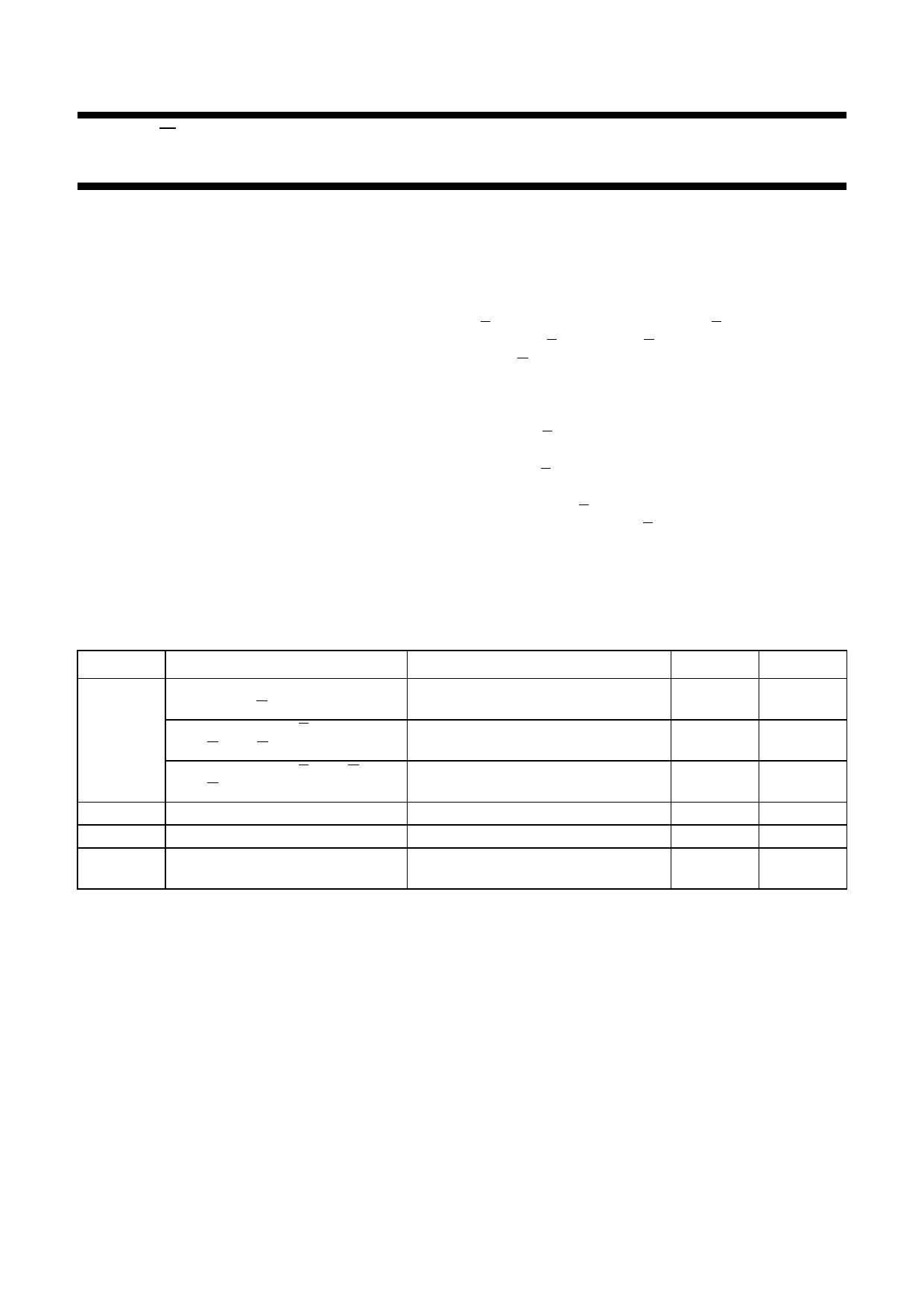
QUICK REFERENCE DATA
GND = 0 V; Tamb = 25 °C; tr = tf ≤ 2.5 ns.
SYMBOL
PARAMETER
tPHL/tPLH
fmax
CI
CPD
propagation delay nCP to nQ
and nCP to nQ
propagation delay nSD to nQ
and nRD to nQ
propagation delay nSD to nQ
and nRD to nQ
maximum clock frequency
input capacitance
power dissipation capacitance per
flip-flop
CONDITIONS
CL = 50 pF; RL = 500 Ω; VCC = 3.3 V
CL = 50 pF; RL = 500 Ω; VCC = 3.3 V
CL = 50 pF; RL = 500 Ω; VCC = 3.3 V
CL = 50 pF; RL = 500 Ω; VCC = 3.3 V
notes 1 and 2
Notes
1. CPD is used to determine the dynamic power dissipation (PD in µW).
PD = CPD × VCC2 × fi × N + Σ(CL × VCC2 × fo) where:
fi = input frequency in MHz;
fo = output frequency in MHz;
CL = output load capacitance in pF;
VCC = supply voltage in Volts;
N = total load switching outputs;
Σ(CL × VCC2 × fo) = sum of the outputs.
2. The condition is VI = GND to VCC.
TYPICAL
UNIT
3.8
ns
3.2
ns
3.5
ns
330
MHz
5.0
pF
23
pF
2004 Mar 18
2
Share Link: 