AD7273 查看數據表(PDF) - Analog Devices
零件编号
产品描述 (功能)
生产厂家
AD7273 Datasheet PDF : 20 Pages
| |||
PRELIMINARY TECHNICAL DATA
Preliminary Technical Data
CIRCUIT INFORMATION
The AD7273/AD7274 are high speed, low power, 10-/12-
Bit, single supply, analog-to-digital converters (ADC)
respectively. The parts can be operated from a +2.35V to
+3.6V supply. When operated from any supply voltage
within this range, the AD7273/AD7274 are capable of
throughput rates of 3 MSPS when provided with a 52
MHz clock.
The AD7273/AD7274 provide the user with an on-chip
track/hold, A/D converter, and a serial interface housed in
an 8-lead TSOT or an 8-lead MSOP package, which
offers the user considerable space saving advantages over
alternative solutions. The serial clock input accesses data
from the part but also provides the clock source for the
successive-approximation A/D converter. The analog
input range is 0 to VREF. An external reference is required
by the ADC and this reference can be in the range of 1.2V
to VDD.
The AD7273/AD7274 also feature a Power-Down option
to allow power saving between conversions. The power
down feature is implemented across the standard serial
interface as described in the Modes of Operation section.
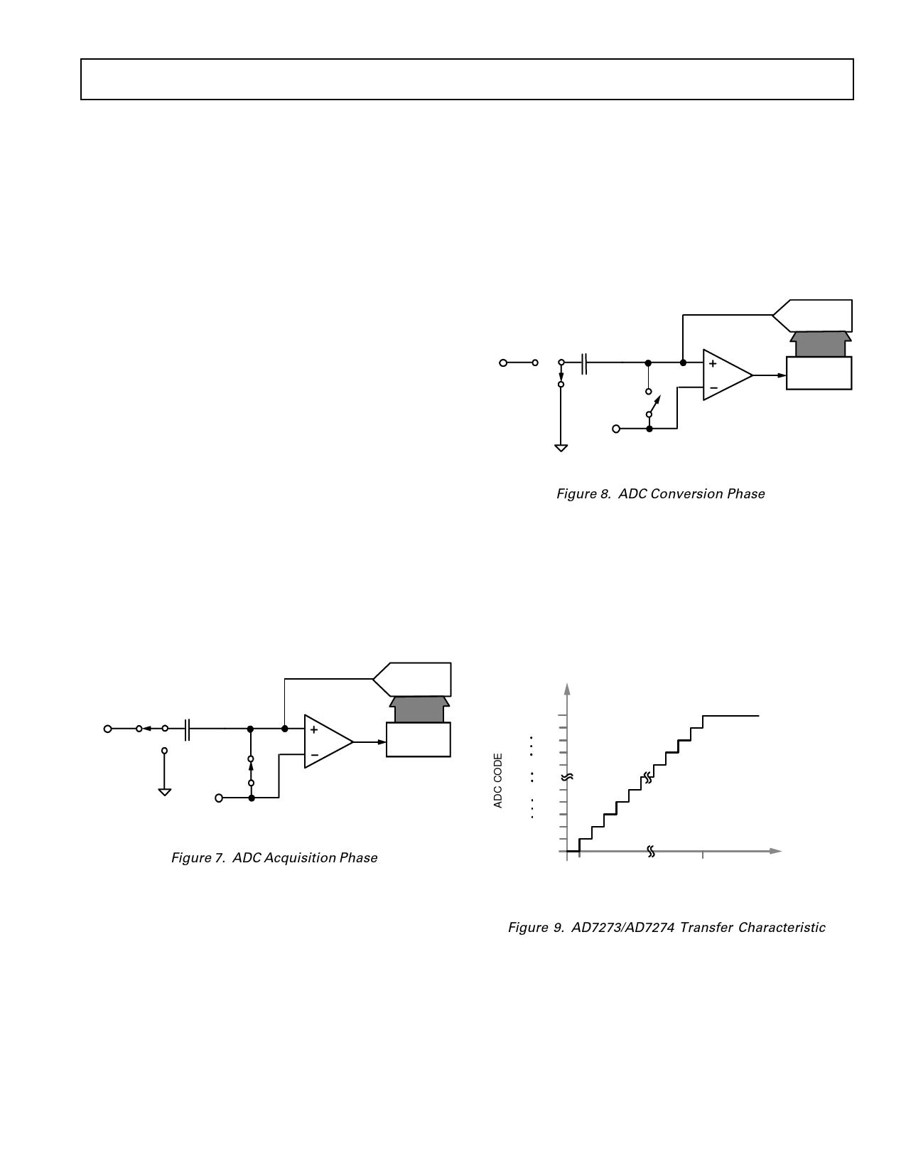
CONVERTER OPERATION
The AD7273/AD7274 is a successive-approximation ana-
log-to-digital converter based around a charge redistribu-
tion DAC. Figures 7 and 8 show simplified schematics of
the ADC. Figure 7 shows the ADC during its acquisition
phase. SW2 is closed and SW1 is in position A, the com-
SAMPLI NG
CAPACI TOR
A
VI N
SW1
B
ACQUI SI TI ON
PHASE
SW2
AGND
VDD / 2
CHARGE
REDISTRIBUTI ON
DAC
COMPARATOR
CONTROL
LO GI C
Figure 7. ADC Acquisition Phase
AD7273/AD7274
When the ADC starts a conversion, see Figure 8, SW2
will open and SW1 will move to position B causing the
comparator to become unbalanced. The Control Logic
and the Charge Redistribution DAC are used to add and
subtract fixed amounts of charge from the sampling ca-
pacitor to bring the comparator back into a balanced con-
dition. When the comparator is rebalanced the conversion
is complete. The Control Logic generates the ADC out-
put code. Figure 9 shows the ADC transfer function.
SAMPLING
A
CAPACITOR
VIN
SW1
B
CONVERSION
PHASE
SW2
AGND
VDD / 2
CHARGE
REDISTRIBUTION
DAC
COMPARATOR
CONTROL
LOGIC
Figure 8. ADC Conversion Phase
ADC TRANSFER FUNCTION
The output coding of the AD7273/AD7274 is straight
binary. The designed code transitions occur midway
between succesive integer LSB values, i.e, 0.5LSB,
1.5LSBs, etc. The LSB size is VREF/4096 for the AD7274,
VREF/1024 for the AD7273. The ideal transfer characteris-
tic for the AD7273/AD7274 is shown in Figure 9.
111...111
111...110
111...000
011...111
1LSB = VREF/4096 (AD7274)
1LSB = VREF/1024 (AD7273)
000...010
000...001
000...000
0V 0.5LSB
+VDD-1.5LSB
ANALOG INPUT
Figure 9. AD7273/AD7274 Transfer Characteristic
REV. PrB
–11–
Share Link: 