PSD834F2-10J 查看數據表(PDF) - STMicroelectronics
零件编号
产品描述 (功能)
生产厂家
PSD834F2-10J
STMicroelectronics

PSD834F2-10J Datasheet PDF : 95 Pages
| |||
PSD834F2V
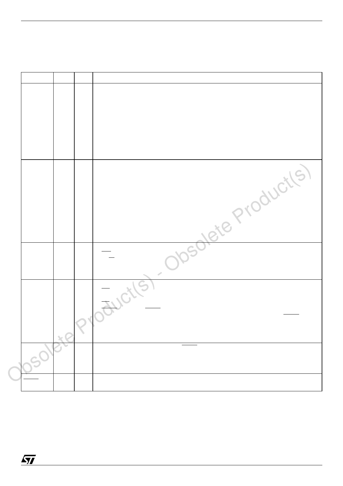
PIN DESCRIPTION
Table 4 describes the signal names and signal
functions of the PSD.
Table 4. Pin Description (for the PLCC52 package - Note 1)
Pin Name Pin Type
Description
ADIO0-7
30-37 I/O
This is the lower Address/Data port. Connect your MCU address or address/data bus
according to the following rules:
1. If your MCU has a multiplexed address/data bus where the data is multiplexed with the
lower address bits, connect AD0-AD7 to this port.
2. If your MCU does not have a multiplexed address/data bus, or you are using an
80C251 in page mode, connect A0-A7 to this port.
3. If you are using an 80C51XA in burst mode, connect A4/D0 through A11/D7 to this
port.
ALE or AS latches the address. The PSD drives data out only if the READ signal is active
and one of the PSD functional blocks was selected. The addresses on this port are
passed to the PLDs.
uct(s) ADIO8-15 39-46 I/O
solete Prod CNTL0 47 I
uct(s) - Ob CNTL1 50 I
lete Prod CNTL2 49 I
Obso Reset
48 I
This is the upper Address/Data port. Connect your MCU address or address/data bus
according to the following rules:
1. If your MCU has a multiplexed address/data bus where the data is multiplexed with the
lower address bits, connect A8-A15 to this port.
2. If your MCU does not have a multiplexed address/data bus, connect A8-A15 to this
port.
3. If you are using an 80C251 in page mode, connect AD8-AD15 to this port.
4. If you are using an 80C51XA in burst mode, connect A12/D8 through A19/D15 to this
port.
ALE or AS latches the address. The PSD drives data out only if the READ signal is active
and one of the PSD functional blocks was selected. The addresses on this port are
passed to the PLDs.
The following control signals can be connected to this port, based on your MCU:
1. WR – active Low Write Strobe input.
2. R_W – active High READ/active Low WRITE input.
This port is connected to the PLDs. Therefore, these signals can be used in decode and
other logic equations.
The following control signals can be connected to this port, based on your MCU:
1. RD – active Low Read Strobe input.
2. E – E clock input.
3. DS – active Low Data Strobe input.
4. PSEN – connect PSEN to this port when it is being used as an active Low READ
signal. For example, when the 80C251 outputs more than 16 address bits, PSEN is
actually the READ signal.
This port is connected to the PLDs. Therefore, these signals can be used in decode and
other logic equations.
This port can be used to input the PSEN (Program Select Enable) signal from any MCU
that uses this signal for code exclusively. If your MCU does not output a Program Select
Enable signal, this port can be used as a generic input. This port is connected to the
PLDs.
Resets I/O Ports, PLD macrocells and some of the Configuration Registers. Must be Low
at Power-up.
11/95
Share Link: